Clear Timer on Compare (CTC) mode is a fundamental operation mode for microcontroller timers. It allows developers to generate precise square wave frequencies by continually comparing the internal timer counter value against a predetermined reference, known as the compare value.
This tutorial explores how to utilize the ATmega328P microcontroller in CTC mode through practical code examples while also contrasting CTC operation with standard timer modes. For broader applications, you can explore more ATmega328p Timer Programming Examples.
Timers and CTC pins
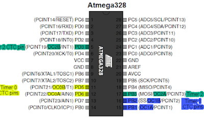
The ATmega328P features three distinct timer/counter modules: Timer 0, Timer 1, and Timer 2. Timer 0 and Timer 2 are 8-bit counters, whereas Timer 1 is a 16-bit counter. Each of these timers includes built-in Clear Timer on Compare Match (CTC) functionality. Equipped with dual compare units, every timer can independently output CTC waveforms on two separate pins. Specifically, Timer 0 controls pins PD6 (OC0A) and PD5 (OC0B), Timer 1 manages pins PB1 (OC1A) and PB2 (OC1B), and Timer 2 drives pins PB3 (OC2A) and PD3 (OC2B). The pin allocations are illustrated below.

Timer 0
For the practical implementation in this guide, we will focus on Timer 0.
Using timer CTC mode offers two primary advantages. First, it gives users fine-grained and highly flexible control over the output frequency of square waves generated at the OC0A or OC0B pins. Second, it greatly streamlines the process of counting and responding to external events.
When configuring Timer 0 in CTC mode, a target count (compare) value is written into either the OCR0A or OCR0B register. Once initiated, the timer increments from zero until it equals the value stored in the respective OCR0x register. Upon hitting this match condition, the corresponding OCF0A or OCF0B flag inside the TIFR0 register is triggered. Developers can choose to either poll this flag directly within a loop to execute tasks like toggling LEDs, reading switches, or sampling data, or configure an automatic interrupt service routine via TIMER0_COMPA_vect or TIMER0_COMPB_vect.
The mathematical formula used to determine the count value required for the OCR0A or OCR0B register is shown below.
\[C=\frac{F_{clk}}{2 N F_{w}}-1\]
where Fclk represents the CPU clock frequency of the microcontroller, N denotes the chosen prescaler value, and Fw stands for the desired output wave frequency.
Alternatively, the equation can be expressed using the square wave time period (Tw) instead of frequency (Fw).
\[C=\frac{F_{clk} T_{w}}{2 N}-1\]
For instance, to generate a square wave with a period Tw = 100 microseconds (equal to a 10 kHz frequency) using an 8 MHz CPU clock and an 8 prescaler, the register count is computed as:
\[C=\frac{8*10^6*100*10^{-6}}{2*8}-1\]
resulting in:
C = 49
Important Registers for CTC mode
Proper configuration of the ATmega328P microcontroller for CTC operation relies on several core registers.
a. TCCR0A – Timer/Counter 0 Control Register A


Phase Correct PWM settings for COM0B1 and COM0B0 are structured as follows:

b. TCCR0B – Timer/Counter 0 Control Register B


c. TIMSK0 – Timer/Counter 0 Interrupt Mask Register

d. TIFR0 – Timer/Counter 0 Interrupt Flag Register

e. OCR0A – Output Compare Register0 A

f. OCR0B – Output Compare Register0 B

Programming Examples of ATmega328p in CTC mode
CTC mode can be implemented using either a polling mechanism or an interrupt-driven approach. Below, we first examine the polling method followed by the interrupt configuration using the OCR0A register.
CTC mode with Polling
The C code snippet below sets up Timer 0 in CTC toggle mode with an 8 prescaler. This configures Port D Pin 6 (OC0A) to output a square wave frequency calculated via the formulas above. Here, the goal is a 10 kHz signal corresponding to a 100 microsecond period. The target pin must be defined as an output using the DDRD register.
# C program code
#ifndef F_CPU
#define F_CPU 8000000UL
#endif

#include <avr/io.h>

void ctcDelay();


int main()
 {
   DDRD |= (1<<PD6);    //make PORT D pin 6(OC0A pin) an output pin

   while (1){
		ctcDelay();
	}

   return 0;
 }


ctcDelay(){
	OCR0A = 49;	//load 49 into OCR0A for delay of 100us
	//configure timer0 for CTC mode with prescalar of 8
	TCCR0A |= (1<<COM0A0) | (1<<WGM01);
	TCCR0B |= (1<<CS01);

	while((TIFR0 &  (1<<OCF0A)) == 0);	//check OCF0A flag
	TIFR0 = (1<<OCF0A);	//clear OCF0A flag
}
Alternatively, the same logic can be adapted for output options beyond the primary OC0A pin. A typical hardware schematic layout for this configuration is shown below.
CTC mode with Interrupt
Alternatively, timer compare matches can trigger interrupts. This requires enabling the Output Compare Match A Interrupt Enable bit (OCIE0A) inside the TIMSK0 register.
#C program code for CTC mode with Interrupt
#ifndef F_CPU
#define F_CPU 8000000UL
#endif

#include <avr/io.h>
#include <avr/interrupt.h>

int main()
 {
   DDRD |= (1<<PD6);

   OCR0A = 49;	//load 49 into OCR0A for delay of 100us
	//configure timer0 for CTC mode with prescalar of 8
	TCCR0A |= (1<<COM0A0) | (1<<WGM01);
	TCCR0B |= (1<<CS01);
	TIMSK0 |= (1<<OCIE0A);	//enable  timer0 output compare match A interrupt
	sei(); 	//set global interrupt

   while (1);

   return 0;
 }

ISR(TIMER0_COMPA_vect){

}
In this interrupt-driven setup, the microcontroller creates a 10 kHz wave (100 microsecond period) using an 8 MHz CPU clock and an 8 prescaler by loading a count of 49 into OCR0A. Standard timer calculation utilities or manual formulas yield this identical value. Implementation requires including
Conclusion
Mastering CTC mode on the ATmega328P provides a robust technique for generating accurate timing and stable square wave frequencies. By understanding the register layouts and configuration steps detailed here, developers can easily implement precise timing into their hardware projects using either polling or interrupt-based designs.